Nanotechnology has been grist for the science fiction mill ever since Nobel Prize-winning physicist Richard Feynman introduced the concept in a 1959 lecture at the California Institute of Technology.
In Arthur C. Clarke’s 1993 novel, The Hammer of God, it’s 2110, and Captain Robert Singh must redirect a meteor from reducing a utopian, nanotechnologically-enhanced earth to rubble. Meanwhile in The Diamond Age (1996, Neal Stephenson) nanotech engineer John Percival Hackworth hunts for a primer on building a supercomputer before it falls into the wrong hands.
In the real world, molecule-sized machines building molecule-sized products have yet to arrive in the consumer market, but the principles behind the theory have already yielded results in pharmaceuticals and biotechnology. The advances are helping to create the next generation of digital x-ray sensors.
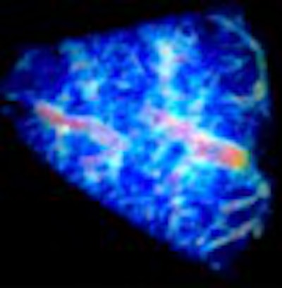
Nanocrystal Imaging, originally founded in 1993 as Nanocrystal Technology, has discovered a process for creating what it calls doped nanocrystals -- nanometer-sized luminescent material with applications for lighting, communications, sensors, and biological tags. The Briarcliff Manor, NY-based firm is using the technology to create phosphor-filled microchannel scintillator plates for converting x-rays to light.
Doped nanocrystals are developed by creating a quantum-confined atom, in which the properties of the localized atom are modulated by the "cage" size (2-5 nanometers) of the crystal containing it. This technique is possible only when the size of the cage is comparable to the diameter of the excited state of the atom.
"The confinement imposed by the nanocrystal modulates the optical property of dopant, and the confinement-induced symmetry fluctuations lead to atomic blinking with several distinct states. Our phosphor’s absorption and emission can be tailored to pure white light," said Nanocrystal Imaging’s CEO, Rameshwar Bhargava, PhD.
Bhargava is a former director of physics and material science and scientific advisor for Philips Research, the R&D arm of the Dutch multinational conglomerate. He incorporated the new firm in October 1997 with $5 million in venture funding. Nanocrystal Imaging now comprises a multidisciplinary team of physicists, electrical engineers, mechanical engineers, material scientists, chemists, and processing engineers.
Because the storage phosphors have been engineered at the nanometer level, the output is producing images with a digital resolution of 15 to 30 line pairs per millimeter. The improved contrast due to the enhanced light output of the technology means radiation doses can be decreased, said Bhargava.
 |
The scintillator plate technology developed by the company can be integrated with complementary metal-oxide semiconductor (CMOS) sensors, charge-coupled device (CCD) sensors, and amorphous silicon sensors for different digital imaging modalities. The company is currently fabricating 2 x 2-inch scintillator plates, and has also processed 4 x 4-inch plates.
The firm has also used the scintillator plate technology to create a camera for recording CT images. The scintillator was combined with an image intensifier, with a variable gain up to 10,000, and was coupled to a CCD sensor. Images were then taken at 50-micron slice thickness and at a lower radiation dose than with conventional CT.
 |
"The camera used in the CT images had a 1-inch plate coupled with an image intensifier. Since we conducted that study, we’ve increased the light output of the plate by at least 100 times, eliminating the use of the intensifier," Bhargava said.
The company is evaluating the use of the technology for the possible retrofitting of current mammography systems. Based on the results of its research, the firm is confident that it can achieve twice the resolution of commercially available digital mammography systems at similar dose rates, and at a lower price. Bhargava also sees potential uses for the scintillator plates in bone-density mapping and cardiac imaging.
The firm is also in the process of obtaining U.S. Food and Drug Administration 510(k) clearance for a high-resolution dental detector it has created. The detector will initially be used for conventional intra-oral dental x-rays, with plans to later incorporate the unit with a panoramic system. The firm is hoping to obtain FDA approval by the summer of 2002, according to Bhargava.
By Jonathan S. BatchelorAuntMinnie.com staff writer
December 13, 2001
Related Reading
Swissray books 30 sales in Q1, October 5, 2001
Hologic secures line of credit, September 25, 2001
GE gets additional clearance for Revolution XR/d, September 5, 2001
Schick moves into the black despite revenue dip, August 7, 2001
Imaging Dynamics gains $1.5 million investment, July 24, 2001
Fischer’s SenoScan closes in on FDA PMA approval, July 23, 2001
Copyright © 2001 AuntMinnie.com